










Desk Report
India opened the next phase of its semiconductor push on Friday, launching the Semicon 2.0 portal for new chip-making applications and approving 12 more electronics component projects worth ₹7,503 crore, with Madhya Pradesh among the seven states that will host the new units.
Union Electronics and Information Technology Minister Ashwini Vaishnaw launched the Semicon 2.0 portal in New Delhi on Friday, opening the application window for three of the six pillars of the programme. On the same day, the government also announced 12 additional approvals under the Electronics Components Manufacturing Scheme (ECMS), a move aimed at deepening India’s electronics and semiconductor manufacturing base and reducing dependence on imports for the parts that go into phones, vehicles, appliances and industrial equipment.
Semicon 2.0 Portal: Three Pillars Open for Applications
The Semicon 2.0 portal will receive applications for Pillar 2, which covers machines and materials; Pillar 3, which covers setting up more semiconductor fabrication facilities; and Pillar 4, which covers strengthening the assembly, testing, marking and packaging (ATMP) and outsourced semiconductor assembly and test (OSAT) industries. The fabrication pillar covers silicon, compound semiconductor, discrete and display fabs, while the machines and materials pillar covers the equipment, chemicals and gases that a chip plant needs to run.
The government has made it clear that the portal will accept only applications that are complete in all respects. Speaking at the launch, Vaishnaw said there was no place for placeholders and frivolous applicants, and that only extremely serious players should participate. The same approach will be followed for applications still awaiting approval under ECMS, with applicants found to be bidding without the required readiness removed from consideration. Under Pillar 2, the programme aims to bring in at least three major equipment makers and five chemicals and gases companies.
The remaining three pillars of Semicon 2.0 — chip design, research and development, and talent development — are not yet open on the portal. The six-pillar programme, approved by the Union Cabinet with a fiscal outlay of ₹1,27,500 crore, is run under the India Semiconductor Mission and covers the full journey from designing a chip to making it, packaging it and finding the people to do the work.
12 New ECMS Approvals: ₹7,503 Crore Investment, 7,127 Jobs
The 12 newly approved projects under ECMS involve a projected investment of ₹7,503 crore and are expected to generate production worth ₹39,045 crore and create 7,127 direct jobs. The approvals cover 10 product segments across components, supply chain products and capital goods, and the projects are spread across seven states: Gujarat, Karnataka, Madhya Pradesh, Maharashtra, Punjab, Tamil Nadu and Uttar Pradesh.
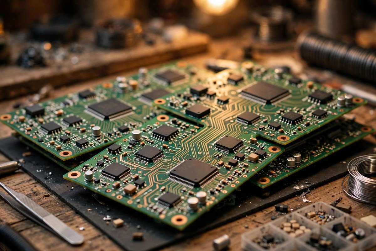
Among the companies receiving approvals are NeST ICELR for multi-layer printed circuit boards, TDConnex (Chennai) for relays, Modern Automotives for heat sinks and Voltix Semicon for speciality ceramics. Indo Asia Copper has been approved for copper foil manufacturing, while TACC and Vidyuta Materials have been approved for anode material and cathode active material respectively. For capital goods, approvals have gone to TDConnex for precision moulds and tooling, Rockwell Automation India for power and control systems, and Wipro Pari Robotics for factory automation and system integration equipment. The product list also includes polypropylene film and camera rims.
Vaishnaw said half of the units approved under ECMS so far belong to small and medium enterprises or micro, small and medium enterprises, underlining that the scheme is drawing in smaller manufacturers alongside large companies. The latest round also marks the first-ever ECMS approvals for copper foil, cathode active material and speciality ceramics — three inputs that Indian electronics makers have largely imported until now.
Madhya Pradesh Among Seven States
For Madhya Pradesh, the announcement adds national momentum to a sector the state has been courting aggressively. The state hosted its own semiconductor summit in Indore on 23–24 October, where Chief Minister Mohan Yadav addressed the inaugural session and investors held one-to-one meetings, and the new central approvals put Madhya Pradesh on the map of states where component manufacturing is set to expand. The announcement did not break down the 12 approvals company-by-company across states, so which specific units come to Madhya Pradesh will become clear as the projects move from approval to groundbreaking.
The inclusion matters because component manufacturing is the layer beneath the headline chip fabs. Printed circuit boards, copper foil, relays, heat sinks and ceramics are the parts that every electronics product needs, and building them in India shortens supply chains for the phone, automobile and appliance factories that already operate in and around the state. A local supply base also means jobs that do not depend on a single large fab, but spread across many mid-sized units.
The Bigger Picture: A ₹1.27 Lakh Crore Programme
With the latest additions, the total number of approved applications under ECMS has reached 118, covering 34 products across 16 states. Together, these projects involve an expected investment of ₹77,051 crore, projected production of ₹5.73 lakh crore and direct employment potential of 81,755 people. ECMS itself is a ₹40,000 crore scheme, and the government said it has received 275 applications under it so far. On closer scrutiny, officials found that nearly 17 to 18 of these applicants did not have the right approvals, technology vendors or other basic requirements in place — the reason the government is now insisting on complete applications only.
The first phase of the Semicon India Programme resulted in the approval of 12 projects across six states, involving cumulative investments of more than ₹1.64 lakh crore. Five of those projects had commenced commercial production by October 2026, the government said, suggesting that the programme is moving from announcements to operating plants. Semicon 2.0 is designed to build on that base, with the new portal channelling applications into the three pillars where India most needs capacity: the machines and materials that fabs depend on, more fabs themselves, and the packaging and testing units that finish a chip.
Stricter Scrutiny for Applicants
The insistence on complete applications is the clearest signal from Friday’s launch. In the first phase, the government found applicants who were bidding for incentives without technology partners or basic readiness, and officials said such applicants would be removed from the list. The message to industry is that the new phase rewards preparation: a company must arrive with its technology vendor, its approvals and its project plan in place, rather than treating an application as a placeholder while it sorts out the details.
That discipline also protects public money. The incentives under ECMS and Semicon 2.0 are tied to investment and production, so a half-ready applicant that never builds would block a slot another company could have used. By filtering at the application stage, the government is trying to ensure that the 118 approvals already given, and the ones that follow through the new portal, turn into factories, production and jobs rather than paper commitments.
What Happens Next
With the Semicon 2.0 portal now open, applications for pillars two, three and four will be received and evaluated, while the remaining pillars — design, research and development, and talent — are expected to open later. The scrutiny of pending ECMS applications will continue alongside, and the approved projects will move towards land, construction and hiring in the seven states named on Friday.
The announcement came on Dhanteras, a day when Indian markets also surged, and it sets up a busy season for the programme: the first test of the new portal will be the quality and number of applications it draws in its opening weeks, and whether the stricter entry bar produces a faster conversion from approval to production than the first phase managed.
Disclaimer: This report is based on available sources and verification. If any fact is found to be incorrect, a correction will be published.